- 您现在的位置:买卖IC网 > Sheet目录473 > MAX2691EVKIT# (Maxim Integrated)KIT EVAL FOR MAX2691
�� �
�
�MAX2691�
�L2� Band� GPS� Low-Noise� Amplifier�
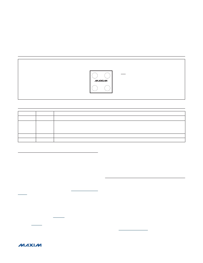
�Bump� Configuration�
�TOP� VIEW�
�+�
�V� CC�
�A1�
�A2�
�RFOUT� (SHDN)�
�MAX2691�
�RFIN�
�B1�
�B2�
�GND�
�WLP�
�Bump� Description�
�BUMP�
�A1�
�A2�
�B1�
�B2�
�NAME�
�V� CC�
�RFOUT�
�(� SHDN� )�
�RFIN�
�GND�
�FUNCTION�
�Supply� Voltage.� Bypass� to� ground� with� a� 10pF� capacitor� as� close� as� possible� to� the� IC.�
�RF� Output/� SHDN� Input.� RFOUT� is� internally� matched� to� 50� I� and� pulled� up� to� V� CC� through� a� 1M� I�
�resistor.� SHDN� is� shared� with� the� RFOUT� bump.� The� device� is� in� active� mode� by� default� once� V� CC�
�is� applied.� RFOUT(� SHDN� )� can� be� pulled� to� a� DC� low� through� a� 25k� I� resistor� to� shut� down� the� IC.�
�RF� Input.� Requires� a� DC-blocking� capacitor� and� external� matching� components.�
�Ground.� Connect� to� the� PCB� ground� plane.�
�Detailed� Description�
�The� MAX2691� LNA� is� designed� for� GPS� L2� applications.�
�The� device� features� a� power-shutdown� control� mode�
�to� eliminate� the� need� for� an� external� supply� switch.�
�The� device� achieves� high� gain,� low� noise� figure,� and�
�excellent� linearity.�
�Input� and� Output� Matching�
�The� MAX2691� requires� an� off-chip� input� match.� Only� an�
�inductor� in� series� with� a� DC-blocking� capacitor� is� needed�
�to� form� the� input� matching� circuit.� The� Typical Application�
�Circuit� shows� the� recommended� input-matching� network.�
�These� values� are� optimized� for� the� best� simultane-�
�ous� gain,� noise� figure,� and� return� loss� performance.�
�Reducing� the� input� coupling� capacitor� results� in� a� lower�
�IIP3.� The� device� integrates� an� on-chip� output� matching�
�to� 50� I� at� the� output,� eliminating� the� need� for� external�
�matching� components.� Table 1� lists� typical� device� S�
�parameters� and� K� f� values.� Typical� noise� parameters� are�
�shown� in� Table 2� .�
�Shutdown�
�The� MAX2691� includes� an� optional� shutdown� feature� to�
�turn� off� the� entire� chip.� The� device� is� placed� in� active�
�mode� by� default� once� V� CC� is� applied,� due� to� the� on-chip�
�pullup� resistor� to� V� CC� at� the� RFOUT� bump� (shared� with�
�the� SHDN� input).� To� shut� down� the� part,� apply� a� logic-low�
�to� the� RFOUT� bump� through� an� external� resistor� with� an�
�adequate� value,� e.g.,� 25k� I� ,� in� order� not� to� load� the� RF�
�output� signal� during� active� operation.�
�Applications� Information�
�A� properly� designed� PCB� is� essential� to� any� RF� micro-�
�wave� circuit.� Use� controlled-impedance� lines� on� all�
�high-frequency� inputs� and� outputs.� Bypass� V� CC� with�
�decoupling� capacitors� located� close� to� the� device.� For�
�long� V� CC� lines,� it� may� be� necessary� to� add� decoupling�
�capacitors.� Locate� these� additional� capacitors� further�
�away� from� the� device� package.� Proper� grounding� of�
�the� GND� pin� is� essential.� If� the� PCB� uses� a� topside� RF�
�ground,� connect� it� directly� to� the� GND� pin.� For� a� board�
�where� the� ground� is� not� on� the� component� layer,� connect�
�the� GND� pin� to� the� board� with� multiple� vias� close� to� the�
�package.�
�Refer� to� www.maxim-ic.com� for� the� MAX2691� EV� kit�
�schematic,� Gerber� data,� PADS� layout� file,� and� BOM�
�information.�
�?????????????????????????????????????????????????????????????????� Maxim� Integrated� Products� 5�
�发布紧急采购,3分钟左右您将得到回复。
相关PDF资料
MAX2693LEVKIT#
EVAL KIT
MAX2694EVKIT#
EVAL KIT MAX2694
MAX2695EVKIT#
EVAL KIT MAX2695
MAX2741EVKIT
EVAL KIT MAX2741
MAX2742ECM+D
IC GPS RF FRONT END 48TQFP
MAX2745ECM+D
IC GPS RF FRONT END 48TQFP
MAX2750AUA+
IC VCO MONO 2.4GHZ 8-MSOP
MAX2752EVKIT
EVAL KIT
相关代理商/技术参数
MAX2691EWS+
制造商:Maxim Integrated Products 功能描述:LOW NOISE FIGURE GPS L2 BAND LNAS IN AN ULTRA SMALL WLP PACK - Rail/Tube
MAX2691EWS+T
功能描述:射频放大器 GPS/GNSS Low-Noise Amplifier RoHS:否 制造商:Skyworks Solutions, Inc. 类型:Low Noise Amplifier 工作频率:2.3 GHz to 2.8 GHz P1dB:18.5 dBm 输出截获点:37.5 dBm 功率增益类型:32 dB 噪声系数:0.85 dB 工作电源电压:5 V 电源电流:125 mA 测试频率:2.6 GHz 最大工作温度:+ 85 C 安装风格:SMD/SMT 封装 / 箱体:QFN-16 封装:Reel
MAX2691EWS+T10
功能描述:射频放大器 GPS/GNSS Low-Noise Amplifier RoHS:否 制造商:Skyworks Solutions, Inc. 类型:Low Noise Amplifier 工作频率:2.3 GHz to 2.8 GHz P1dB:18.5 dBm 输出截获点:37.5 dBm 功率增益类型:32 dB 噪声系数:0.85 dB 工作电源电压:5 V 电源电流:125 mA 测试频率:2.6 GHz 最大工作温度:+ 85 C 安装风格:SMD/SMT 封装 / 箱体:QFN-16 封装:Reel
MAX2691LEWS+T
功能描述:射频放大器 GPS/GNSS Low-Noise Amplifier
RoHS:否 制造商:Skyworks Solutions, Inc. 类型:Low Noise Amplifier 工作频率:2.3 GHz to 2.8 GHz P1dB:18.5 dBm 输出截获点:37.5 dBm 功率增益类型:32 dB 噪声系数:0.85 dB 工作电源电压:5 V 电源电流:125 mA 测试频率:2.6 GHz 最大工作温度:+ 85 C 安装风格:SMD/SMT 封装 / 箱体:QFN-16 封装:Reel
MAX2691LEWS+T10
功能描述:射频放大器 GPS/GNSS Low-Noise Amplifier
RoHS:否 制造商:Skyworks Solutions, Inc. 类型:Low Noise Amplifier 工作频率:2.3 GHz to 2.8 GHz P1dB:18.5 dBm 输出截获点:37.5 dBm 功率增益类型:32 dB 噪声系数:0.85 dB 工作电源电压:5 V 电源电流:125 mA 测试频率:2.6 GHz 最大工作温度:+ 85 C 安装风格:SMD/SMT 封装 / 箱体:QFN-16 封装:Reel
MAX2692EVKIT#
功能描述:射频开发工具 MAX2692 Eval Kit RoHS:否 制造商:Taiyo Yuden 产品:Wireless Modules 类型:Wireless Audio 工具用于评估:WYSAAVDX7 频率: 工作电源电压:3.4 V to 5.5 V
MAX2692EWS+
制造商:Maxim Integrated Products 功能描述:- Rail/Tube
MAX2692EWS+T
功能描述:射频放大器 WLAN/WiMAX Low-Noise Amp RoHS:否 制造商:Skyworks Solutions, Inc. 类型:Low Noise Amplifier 工作频率:2.3 GHz to 2.8 GHz P1dB:18.5 dBm 输出截获点:37.5 dBm 功率增益类型:32 dB 噪声系数:0.85 dB 工作电源电压:5 V 电源电流:125 mA 测试频率:2.6 GHz 最大工作温度:+ 85 C 安装风格:SMD/SMT 封装 / 箱体:QFN-16 封装:Reel